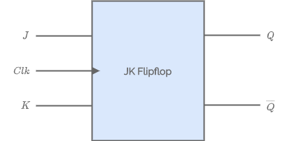
The JK Flip flop can be viewed as a modification of the SR Flip flop. The intermediate state in a JK Flip flop is more refined and precise than that of an SR Flip flop.

Design of JK Flip flop
The design of a JK Flip flop is similar to that of an SR Flipflop. The output is connected back to the input of NAND gate
and
output is connected back to the input of NAND gate
.

Working of JK Flip flop
When is 1 and
is 0, the
output goes 1 on the triggering edge of the clock pulse, and the flip-flop is SET. When
is 0 and
is 1, the
output goes 0 on the triggering edge of the clock pulse, and the flip-flop is RESET.
When both and
are 0, the output does not change from its prior state. When
and
are both 1, the output of the JK flip-flop will toggle between 1 and 0. This is called the race-around condition in a JK Flipflop. This is described in the following truth table.
| 0 | X | X | |
| 1 | 0 | 0 | |
| 1 | 0 | 1 | 0 |
| 1 | 1 | 0 | 1 |
| 1 | 1 | 1 |
Truth table
| 0 | 0 | 0 | 0 |
| 0 | 0 | 1 | 0 |
| 0 | 1 | 0 | 1 |
| 0 | 1 | 1 | 1 |
| 1 | 0 | 0 | 1 |
| 1 | 0 | 1 | 0 |
| 1 | 1 | 0 | 1 |
| 1 | 1 | 1 | 0 |
Characteristic table
| 0 | 0 | 0 | X |
| 0 | 1 | 1 | X |
| 1 | 0 | X | 1 |
| 1 | 1 | X | 0 |
Exctitation table
Expressions for ,
and
can be obtained from the table using the K-Map technique as follows.

